

By Fatemeh Rezaeifar
When I was 18, I left my home in Iran and moved to Japan by myself to start college after being nominated by a Japanese government scholarship. You can imagine how amazed I was by Japan, a country so different from my own. At the University of Tokyo (Todai), I was the only female international student in my class. I remember discovering how an oscilloscope works, learning about transistors and scary high voltage equipment in the lab! Even though our experiments were limited to reproducing previous work with zero discoveries at the state-of-the-art level, I was so excited to learn new things and I wanted more.
I was interested in the physics of electrical discharge in MEMS devices and the lab was under the supervision of the only female faculty member at Todai, professor Akiko Kumada of the High Voltage Engineering Laboratory. She was one of my role models, and she inspired me to go on to graduate studies. Right after my MS defense meeting, I told myself that this small research experience couldn’t be the end of my academic life! I was determined to pursue a PhD in electrical engineering.
"International students could benefit from a course on understanding the unique education system and academic values in the United States."
By this time, I was already used to the Japanese seniority system and I am still amazed by the culture of teamwork in Japan. Everything was well organized and I enjoyed observing science and technology in the world around me; From walking in Akihabara electric town in Tokyo to riding on a fascinating Japanese bullet train (Shinkansen) that connects Tokyo to Osaka - 313 miles in just 2 hours! Nonetheless, I looked to the United States as the next destination on my academic journey.
I started that journey with some advice from my MS research adviser and life mentor, professor Kunihiko Hidaka. Before I left Japan, over some delicious sushi, he gave me advice that I have never forgotten: “Fatemeh San!” (San is a respectful way of calling a person in Japanese and it was very nice of him to use it) “Here in Japanese academics, we don’t strongly criticize a student’s research in front of others, so you haven’t had a chance to experience scientific aggressiveness. Outside Japan, welcome this opportunity head-on and be ready to defend your own work vigorously.”
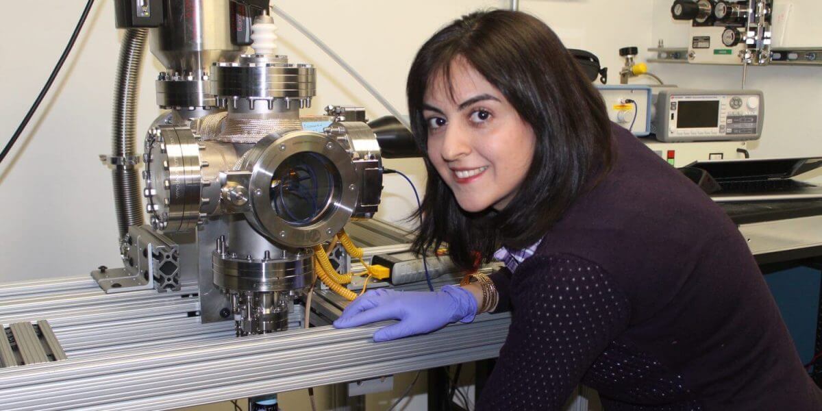
Fatemeh in the USC Cleanroom with her integrated electron emission device. Photo Credit: USC Viterbi
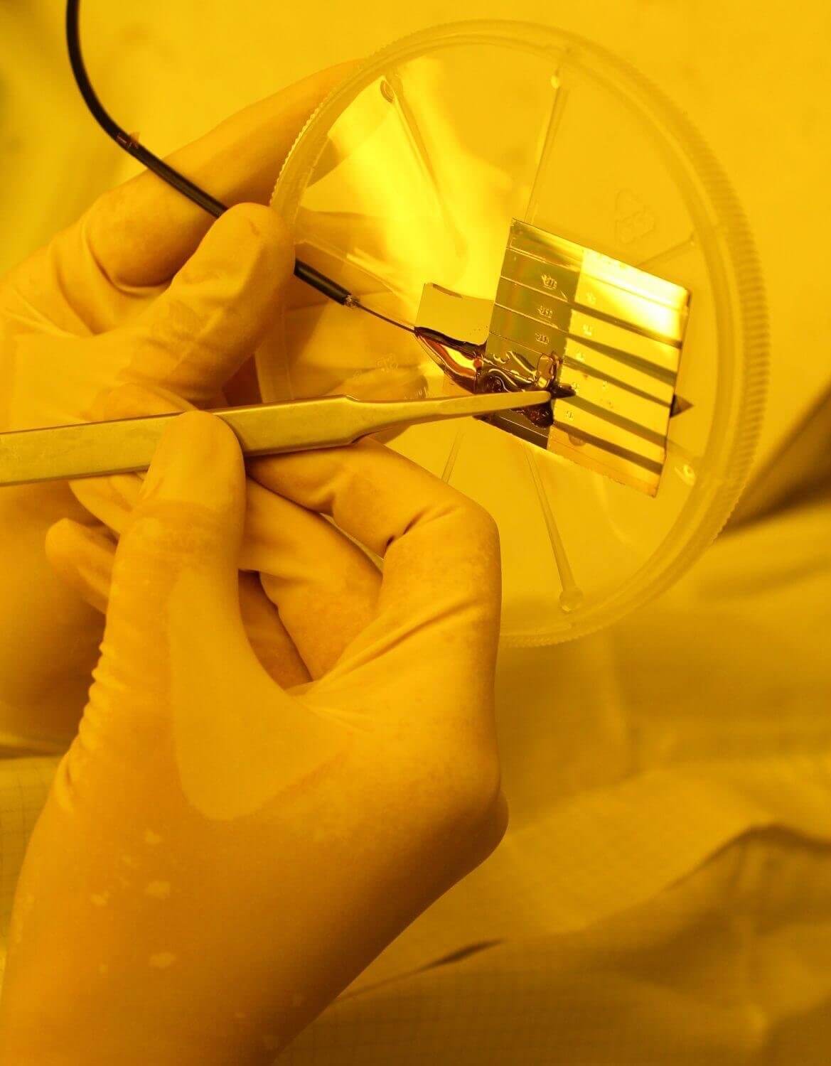
Close up of the integrated electron emission device. PHOTO CREDIT: USC Viterbi
With that in mind, I began my PhD work at the Ming Hsieh Department of Electrical Engineering at USC. I soon had a better understanding of his advice! I had to quickly learn to present my own ideas and defend my work. At the same time, I was participating in amazing research in the field of integrated photonics, design and characterization. As a new PhD student, I was learning to deal with limitations and the practice of finding solutions with possible options to achieve a goal. The skills and advice that makes PhD life much easier! I believe international students could benefit from a course on understanding the unique education system and academic values in the United States. Becoming familiar with these differences can help us be more strategic, take advantage of opportunities to focus on our PhD project, and move our dissertations forward smoothly.
In searching for a novel challenge to tackle as my PhD project, my adviser, Rehan Kapadia, proposed utilizing an integrated photonics approach for high-speed and high power electron emission devices. These devices will mainly be used for defense, imaging, sensing and electronics applications. Specifically, vacuum electron devices, high-powered THz generation source, free-electron laser source, time resolved electron microscopy to capture images from ultrafast reactions are relevant active fields of research. The integrated photonics approach had never been considered for these applications previously. As such, we had to evaluate the enhancement in efficiency as well as the transient response of the integrated photonic approach.
At the time, I would never have guessed that this two-year endeavor would end with major AFOSR funding, a first prize at the EE department research festival, and a completely new piece of technology built by my own hands entirely in our lab.
First, I designed the main components for our device’s “optical cavities” that provides enhanced interaction between light and emitting material and evaluating the transient response of the emitter. After 6 months of optical re-design and evaluation, Dr. Kapadia and I concluded that the approach was promising and he was successful in getting AFOSR funding for us. By that time, we had two heads full of ideas and a brand new lab space to conduct our research!
For the next 6 months, my focus was on building and testing an ultra high vacuum (UHV) system capable of getting to 1e-8 Torr in 2 hours and delivering optics inside a vacuum chamber. I had to learn tons of new skills from how to deal with forever-spinning screws to a bake out technique for achieving UHV and finding appropriate optical and electrical generation and detection equipment. As an experimental researcher, the process of making and getting things to work from scratch was new for me and I appreciate my adviser’s help and advice.
"Developing the entire process, loading the sample into the vacuum chamber and finally detecting a photocurrent assisted via integrated waveguide was the best moment of my entire graduate school experience."
Finally, after verifying our characterization setup using a graphene emitter on a sharp tip silicon array (which we fabricated in USC’s cleanroom), I had the confidence to start developing a layout and fabrication procedure for producing a prototype integrated emission device, which included a graphene emitter on a silicon nitride waveguide. Later I worked on a platform to couple a laser from fiber on V-groove to optical waveguide. Developing the entire process, loading the sample into the vacuum chamber and finally detecting a photocurrent assisted via integrated waveguide was the best moment of my entire graduate school experience. The feeling of delivering results in independent and novel research has been extremely self-fulfilling.
I encourage girls not to give up their dreams with failure. Fight to overcome difficulties, understand and learn from cultural differences and convert obstacles into victory. As Noel Coward said, “The secret of success is the capacity to survive failure.”
Fatemeh Rezaeifar is a PhD student in Dr. Rehan Kapadia’s Laboratory for Photons, Electrons, and Materials. She won first place at the 2017 EE Research Festival for her work in this story. See the presentation of her winning research here.
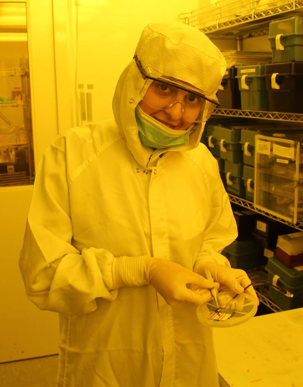
Step 1: Get Cleanroom Ready
Step 2: Fabricate The Prototype!
Step 3: Laser Coupling in Device
Published on January 11th, 2018
Last updated on March 30th, 2021